Power-One Power Supply Hackers Page
Note:
To access the ExpressPCB .PCB and .SCH files for this page, use this
.ZIP archive. Each .SCH and .PCB
link below also links to the same .ZIP file.
-- Dave
Power-One has built open frame linear power supplies since the 70's.
These workhorses have been built nearly the same way for so many
years, and there are many available on the new and surplus markets.
The design is simple enough, the technology is understandable to
someone with basic electronics background. In other words they are
ideal for hacking. What can be done with them? In addition to using
them to learn about power supply theory, I have hacked many power
supplies and find these to be fun and easy. I describe simple hacks
from adding a meter or two, widening the voltage range, coaxing them
to do adjustable current limiting. All these can be done with a few
external parts. My grand finale is to eliminate the ancient uA723
regulator and replace it with a proper full range, precision voltage
/ current limit design with good precision monitors and even a PC to
control and monitor it.
Modified, they can be used as lab supplies, battery chargers, or any
place a lab supply is needed. They can even be scavenged for parts
or better still, subsections, they can be re-packaged into a
different chassis.
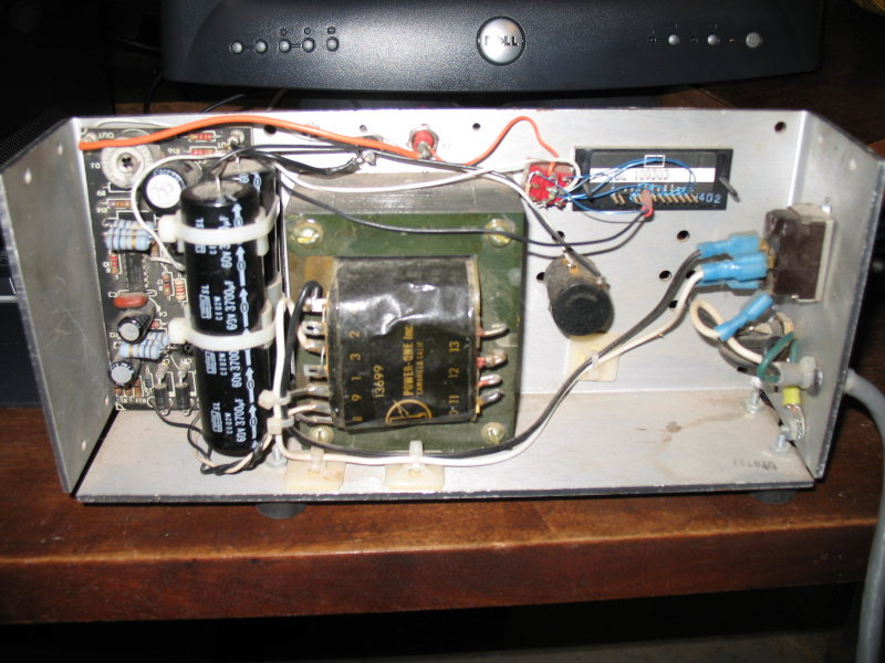
Here is a 24V 2A supply that I hacked years ago and have used as a
lab supply ever since. I set the voltage range to 4V to 25V, removed
a second board and drilled the chassis to make room for the AC line
cord, switch and fuse, binding posts, and a Digital panel meter and
10 turn pot. I mounted rubber feet on the bottom to keep it from
scratching up the bench and also to isolate its heat from the bench.
If I did it again, I would add a separate panel for these additions
and leave the original board intact. It provided useful +/-5VA
outputs.
Each Power-One supply has everything that a linear power supply
needs: An unregulated DC power source, an output stage capable of
dissipating some power, a regulator containing a reference voltage,
a difference amplifier and a current limiter. After 35+ years they
all still use the DIP version of the venerable uA723 Voltage
Regulator. What else do they all have in common?
- Raw DC supply: AC Transformer, diodes and filter capacitors
- AC can be 100, 120 or 240V, 50 or 60Hz
- Beefy TO-3 power transistors, 2N3055 or equivalent, or power
darlingtons
- Current limiting, generally foldback
- Output voltage adjustable over a narrow range, typically ±
15%
- Some power (efficiency) management, usually a boost supply a
little higher than the main supply
- Sturdy 3 or 4 sided 1/8" aluminum chassis
- Voltages from 3.3V to 28V and higher. Most common are 5, 12,
15, 24, 28V
- Remote sense for higher current versions
- Some are unregulated
- Currents from <1A to 50A
- Single, dual (sometimes +/-) and triple configurations
- Overvoltage protection as an option, sometime on a separate
board
Condor and International Power also build nearly identical supplies.
Other manufacturers may also. When you are searching for a supply on
Ebay, use all the vendor names in your searches. The differences are
subtle, if any.
Caveats:
Needless to say this page is not sanctioned by any power supply
manufacturer. By disassembling and modifying a supply you will of
course void the warranty, and you may never be able to get your
power supply back to its original splendor. You may even blow
something up. These things operate from raw AC line voltage which
can be LETHAL. I *STRONGLY* recommend that you:
Insulate all AC wiring with heat
shrink or electrical tape
Add a power switch and fuse of the correct value
Be careful when operating these or any power supplies
Regarding efficiency, linear supplies are quite inefficient, and
therefore burn holes in the ozone layer, cause more coal-burning
power plants to be built, and speed the decline of civilization.
They are fine for low power applications or occasional use such as a
lab supply. But if you're going to keep any power supply heavily
loaded for long periods of time, please do the environment a favor
and use a nice efficient switcher. Your electric bill will also
appreciate it. While you're at it, replace your antique incandescent
light bulbs with modern bulbs. Each bulb saves more power than a
typical linear supply wastes.
The Supplies
Here is a simplified circuit of a Power-One supply. This is a +15V,
3A supply similar to the HC15-3. 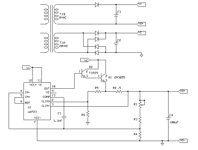
Here is the full schematic of the
HC15-3 in ExpressPCB format as well as in .PDF.
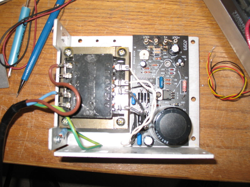
Here's a photo of a HC15-3 below.
You can get ExpressPCB's excellent software for free at www.expresspcb.com.
Most units have current sense resistors to enable current limiting.
These are typically 2-3Watt power resistors, less than 1 ohm, wired
from the output transistor's emitter to the supply output. Some
supplies use 2 or more resistors in parallel to achieve low
resistance and higher power ratings. The resistors are connected to
the current sense pins on the uA723. These inputs are simply the
base and emitter of an internal transistor. When the voltage from
pin 3 to pin 2 exceeds about 0.65V, the internal transistor
conducts, and pulls the output down. I discuss the details of this
further on.
Higher current supplies use multiple output transistors in parallel.
To achieve proper current sharing, each transistor has its own
emitter resistor. Without the resistor, the hottest transistor would
have the lowest Vbe which would cause even higher collector current,
causing it to get even hotter. This effect is called thermal runaway
and ultimately can cause failure of an output transistor as it hogs
all the supply current. Emitter resistor help to balance these
currents. When multiple transistor and emitter resistors are used,
the current limit sense is taken from a single resistor with the
assumption that the currents are all close to the same.
Most supplies have an extra 'boost' supply which is typically a
half-wave rectifier and cap that provides a bit more voltage than
the main supply. This is to provide the few extra volts that the
regulation circuit and output transistor requires without increasing
the main supply. If the main supply were simply increased, the
output transistor would need to burn the power from that extra
voltage drop. Lower voltage supplies simply double the V+ with an
extra diode and cap. Some like the one below use a 'bootstrap'
approach where a separate winding of the transformer provides a
7-10V DC extra voltage. This voltage is connected in series with the
supply output, thus providing a voltage equal to 7-10V more than the
output voltage.
Most are built around single-sided phenolic PC boards.The usual
mounting method is via the TO-3 transistor mounting screws. The
board can be removed by:
Unsoldering the pins of all T0-3s
with a solder-sucker
Removing the screws that mount the T0-3s.
Carefully seeing where all the insulation hardware goes so you can
replace it later.
Some newer units use socket pins for the TO-3s, so you don't need to
unsolder the transistor to remove the board.
Remote voltage sense is provided on some supplies. Look for an extra
pair terminals near the voltage output terminals. Remote sense is a
"Kelvin" or 4-wire connection used to compensate for voltage drop in
the power wiring by sensing the voltage at the load instead of at
the power supply. A second pair of terminals is provided, and these
are wired to the remote load. These terminals are used by the supply
to measure the output voltage, so the + side is typically the
voltage feedback to the voltage divider, and the - side is the V- or
GND terminal of the uA723. Low value resistors are provided between
each sense terminal and its power terminal so that the supply will
still operate when the remote sense inputs are disconnected. The schematic of the HC15-3 in .PDF shows
this.
Over-Voltage Protect is provided on some supplies. It is also called
a "Crowbar" because it shorts the output of the power supply in the
event of a fault that increases the output voltage too much. For
example, on a +5V supply, the overvoltage is set to about +6.2V.
This is implemented with an SCR and voltage sense circuit consisting
of a Zener diode and resistors. When the voltage increases, the SCR
turns on and shorts the output of the supply. If the supply is
functioning it will current limit. If the supply's output transistor
has shorted, the current limit won't function, and the AC fuse
should blow due to a direct short on the power supply.
Some supplies use circuitry on the board for this. Some use an
external board wired to the output terminals. When hacking a supply,
you typically don't want it to ever crowbar, so I recommend
disabling the overvoltage circuit. This can be done by simply
disconnecting an external overvoltage, or by removing the SCR on the
on-board types. The SCR is typically a TO-220 device located near
the outputs. Unsolder and unscrew it, or clip its leads.
uA723
The uA723 (same as the LM723) voltage regulator has been around
since the 60's. It is the core, the brain, the technological center,
if you will of each Power-One supply. It contains all of the
building blocks of a voltage regulator: voltage reference,
difference amplifier, power stage, and current limiter. Below is a
block diagram, courtesy of TI. Here is the uA723 full data sheet.
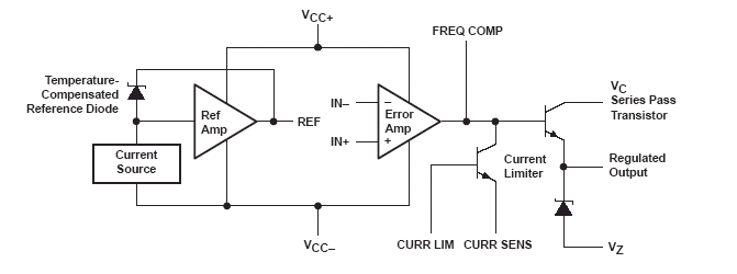
This IC is very flexible and low cost. But it does have limitations.
The voltage reference is nominally 7.15V. The minimum power supply
to make this reference and the rest of the device operate is about
+12V. The maximum voltage is +40V.
The inputs of the difference amplifier have a minimum (common mode)
voltage range of +2V. This means that the output voltage cannot
easily go below +2V without playing games. Most Power-one supplies
operate these inputs between +5V, the lowest standard voltage output
available, and the +7V reference. In fact there is a spec in the
'723 data sheet that says that the + and - inputs must see no more
than +/- 5V. So keep these signals between 2V and the 7V reference.
The '723 output voltage can be about 2.5V below the V+ and VC pins.
Internally, the '723 uses a current source followed by two emitter
followers and can output a maximum of 150mA. In Power-One supplies
this is used to drive external TO-3 output transistors that boost
this to a couple of amps. Most supplies use a 2N3055. The minimum
beta (current gain) of a 2N3055 is about 25, so this 150mA could
theoretically be amplified to about 25 x 150 = 3.75A in a single
TO-3. It is a bad idea to operate the '723 at this maximum current,
and 50 mA is more reasonable maximum. The maximum power of the '723
is about .75W, and at 150ma this only allows .75W / .15A or 5V of
drop between the V+ and the output. Most power-one supplies operate
at fairly high voltage drop.
For example, the +15V 3A supply that I have uses another transistor,
a TO-220 TIP29 between the '723 and the 2N3055. Figure the TIP29 has
an additional beta of 25. So the '723 provides 3A / (25 * 25) or
only 5mA. Another supply I own uses a darlington output transistor
type 2N6059 to provide the higher current gain required.
To identify if your supply uses Darlingtons or vanilla NPNs and
assuming you can't just read the number off the TO-3 and find a data
sheet, load the supply with a nominal load (~0.5 A) and measure the
voltage drop from the base to emitter terminals of the TO-3. If you
get 0.6 to 0.8V, it's a single transistor. If you get 1.1 to 1.5V
it's a darlington.
About 2 or 3 amps is the maximum you want to draw from a single TO-3
without forced air cooling. A 2N3055 is rated for 60V, 10A and 115W,
but 115W is only under ideal conditions: with an infinite heat sink
and at 25C. Lower current, up to 5A, Power-one supplies have only
the aluminum case as the heat sink. Larger supplies up to 50A often
use additional finned heat sinks and encourage forced air cooling.
Needless to say a 50A linear is a generally bad idea due to the
power waste or hundreds of watts at full power.
I estimate the case heat sink to have a thermal resistance of about
3 degrees C / Watt without a finned heat sink and without forced air
cooling. To keep the temperature rise to +50C (+25C ambient = 75C,
quite hot!) , the transistor can dissipate 50C / 3C/W = ~17 Watts.
At 3A, the transistor can only drop 17W / 3A = ~6V.
If you modify a supply and want to operate at lower voltages, you
will drop much more voltage across the transistor and burn more
power. Lets say you want to operate a +15V, 3A supply at +5V. At the
same 3A, the output transistor will burn (15V -5V) * 3A = 30W more.
The additional temp rise at 3C/W is +90C. Ouch! Without forced air
cooling you will need to derate the current of the supply by 1/3 to
1/2. It's a bit counter-intuitive: this supply will output 3A at its
full +15V, but at 5V only lower currents.
Keep in mind that the transformer / cap / diodes can still provide
the full 3A at any output voltage. For that +15V 3A supply, they
provide an unregulated +20V or so at 3A or 60W. The unregulated
parts don't care if most of the 60W is being dissipated on the heat
sink or in an external load. Well, they do care a bit since they
also are mounted to the same heat sink, and when it gets hot, so do
they.
Another way to manage more heat is to remove the T0-3 transistor(s)
and move to a larger, external heat sink. The device can be removed
and simply wired via the traces on the board to the transistor
located within 6-12" away. Once you do this, the Power-One case is
no longer needed: remove the board and transformer and mount them
wherever you want. After removing all the parts, you could even saw
the case in pieces to give you separate brackets for mounting the
transformer and the board and/or heat sink. If you do this, there
are things to watch for: the 2 (or more) transistor screws are the
board mounting. This is convenient if you have a transistor and
insulator, but not convenient if you moved them elsewhere. Since
these transistor connections are still electrically hot, you need to
use insulated washers to mount the board to anything conductive.
Also on some designs, the 2 screw leads of the TO-3 are used as
electrical connections on the board. Once you remove the transistor,
these connections no longer exist. If you see traces on the board
connected to both screw mounts, solder a wire from one screw mount
to the other.
Increase the Voltage Range
Before you do the voltage range mod or the constant current mod,
realize that both of these will cause a larger voltage drop across
the power transistor at high currents. This is the main source of
power and therefore heat in the supply. Get the transistor too hot
at too high a power dissipation, and it will fail, usually by
shorting its collector-to-emitter. This causes the supply to output
its full unregulated voltage. Since you don't want this to happen,
it is important to watch the maximum temperature at high loads, and
particularly at low voltages. There are 2 basic ways to keep it
cool: one is to apply forced air via a fan. The second is to limit
the current at low voltages.
The voltage output of a Power-one is set with resistors and a
trimpot. Older units use a big metal trimpot and newer ones use
smaller plastic ones. Depending on whether the supply is rated for
>7V or <7V, the circuit is wired differently. For Vout >7V,
the +7V reference pin is wired directly to the + input. A resistive
divider with the trimpot reduces the output voltage to 7V to be
applied to the - input. The trimpot allows the output to be
accurately set and allows for some adjustment range. (Sometimes a
single supply is rated for either 12V and 15V operation and the trim
is used to set the voltage. These are typically derated for lower
currents for +15V operation than for 12V.)
For voltages <7V (usually 5V) , the Vout is wired directly to the
- input and the reference is attenuated to the output voltage by a
divider and trimpot.
The >7V supplies are easier to hack. One thing you typically want
is a wide output voltage range. I like to use the 15V or 24V
supplies at 2 or 3 Amps to build lab supplies. I want the output to
go all the way to 0, but the '723 won't allow this easily. The '723
spec is +2V but I like margin and don't often need to go below
+2.5V. To do this, attenuate the reference from +7.15V to +2.5V by
adding two resistors. The resistor ratio is (7.15 - 2.5) / 2.5
or1.86 : 1.00. 1.00K to ground and and 1.87K to the reference will
work. Now the output divider can go from 2.5V to slightly higher
than its rated V. So for a +15V supply, lets push it up to +16V. The
divider here is (16V - 2.5V) / 2.5V or 5.40:1 The large value is a
pot or trimpot, so pick its value first and select the small one to
match. For 16V, a 10K pot will draw <1.6ma of output current and
<25mW. We probably want to use a 10 turn pot and these are
readily available. One turn pots don't allow adjustment to 3 1/2
digits easily. Some people don't like 10 turns since in a panic they
take a long time to turn down, so you could use a 10K, 1 turn in
series with a another 1K in a coarse / fine arrangement. Set the
fine pot to mid scale, adjust the coarse to get close, and then
tweak the fine. The total 16V range here would be 11K, not 10K.
So 10K * 1 / 5.4 is 1852 ohms Use a 1.82K ohm 1%. Mount the pot(s)
and the panel meter(s) on a scrap of sheet metal which can be
mounted to the supply or mounted remotely. Remove the resistor in
series with the PowerOne voltage trimpot and the low side resistor.
Depending on your unsoldering skills you may remove the trimpot too.
Replace the low divider resistor with the 1.82K, and the pot plus
the other resistor with 2 wires. Then run wires to the
external 10K pot. Remember to wire the unused (CCW) terminal to the
wiper for safety in case your pot wiper gets noisy and
intermittently opens up. This will cause the supply to go to +
infinity which is likely to do bad things to a load. This schematic of the HC15-3 shows the
original circuit plus the changes.
If your new supply range is >19.99V, it cannot be displayed on a
3 1/2 digit meter at full resolution. So either use a 199.9V range
and only have .1V of resolution, or add a range switch to the meter
so at lower than 20V you can get 0.01V resolution. This is what I
did on my first supply.
Current Limiting
In order to accurately limit current, it is generally required to
measure the voltage across a low value resistor in series with the
load. If this voltage exceeds a preset limit, then the supply
outputs reduced voltage until the current drops to a safe value.
Power-One supplies do this with a single NPN transistor in the '723.
Its emitter is tied to the power supply voltage output and its base
goes to a current sense resistor. In this way, if the voltage across
the sense resistor increases to about +.7V, the transistor begins to
conduct, reducing the output voltage. This is a crude current limit,
intended to protect the power supply from a short circuited output
load. However, this type of current limit causes the output
transistor to dissipate the full voltage and current which is a
large value of power, causing it to overheat and possibly fail. So
an improved method is needed. This is called foldback current
limiting. With this approach, when a supply goes into current limit,
the current is reduced to a safe value, typically 1/2 or 1/3 of the
limit value. removing the load allows instant recovery.
The '723 can be outfitted for foldback by simply adding a resistor
divider to the current sense input such that as the output voltage
drops, the current threshold also drops. This basic circuit is shown
above. Another problem with this circuit is that it depends on an
uncompensated Vbe voltage which varies about -2mV/ degree C. And
also without varying the low-value current sense resistor, there is
no easy way to reduce the current limit value. However, Power-One
has come up with a clever solution, shown in the schematic of the HC15-3. Note the
current limit trimpot, and how it is connected to the base of the
output transistor, not directly across the current sense resistor.
In this way, the sense resistor plus the output transistor's Vbe are
being measured. These are compared to the trimpot voltage plus the
723's current sense transistor Vbe. Since the Vbe's kind-of cancel
out, the voltage across the shunt is compared to the voltage across
the trimpot. By reducing the trimpot's resistance, the current limit
can be reduced also. The pull-down resistor and diodes provide
current to the trimpot and tailor the foldback current limiting
characteristics. Very clever.
However, for a lab supply, a precision constant current mode is more
desirable than current foldback. In constant current, a control is
used to adjust the maximum output current of the supply, and the
supply will dutifully and accurately output this current at any
voltage from 0V up to the voltage setting. To do this accurately
requires an accurate measurement of current, a precision setting,
and a control loop to take over the power supply when the current
limit is reached. But the Power-One circuit can be easily hacked to
provide a decent if not super-accurate current limiter. To eliminate
the foldback limiting and allow constant current control, all that
is necessary is to regulate the voltage across the trimpot by
regulating the current through the trimpot. This can be done by
replacing R6 and its 2 diodes with a 1mA constant current source to
ground. Now, the 500 ohm trimpot will have a maximum of 1mA * 500 =
0.5V, the maximum voltage desired across the shunt resistor. By
varying the trimpot down, the voltage across the shunt is also
reduced. This circuit isn't perfectly precise, but can be set to any
desired value from about 10% to 100% of the supply's current rating.
It will drift a bit as the power transistor heats up though. But
it's a lot better than nothing and can be used for many
applications. I built this up and found that the Vbe of the current
measuring transistor was a stable 646mV. But the Vbe of the 2N3055
varied quite a bit with current: from about 0.5V at 0 current to
0.8V at 2.5A current. The 0.5V came as a surprise to me. This caused
the minimum current setting to be about 0.3A, not 0 as I had hoped.
The shunt resistor in the HC15-3 was 0.12 ohms. With this change the
current could be varied from 0.3A to about 2.3A. And it was pretty
stable when in current limit.
For a 1mA current source, the National LM334 can be used. It is a
resistor-programmable current source in a TO-92 package. A single 68
ohm resistor is used to set its current. You may have to mess with
the 68 ohm resistor value to get the current ranges you want.
This is a crude variable current limiter. A precision one is shown
below.
Output Monitoring
To monitor and adjust voltage, a DMM can be used across the output
terminals. Current monitoring with a DMM can be done two ways: 1)
Wire a DMM in current mode in series with the output, or 2) Monitor
the voltage across the shunt resistor and solve ohms law.
Low cost 3 1/2 digit LCD and LED digital panel meters (DPMs) can be
hard-wired to serve these functions. For voltage monitoring, use a
5V common ground (not a 9V) compatible DPM. Wire its input as a
19.99V or 199.9V range and set the decimal point accordingly. I like
the All Electronics PM-128E for this application. It is flexible and
cheap ($12.25). It needs a +5 supply at low current. I cheated on
one system and used the +7.1V reference to power the DPM. It has
worked for years, but I suspect that that DPM was specified to
operate from +7V. A better solution is to use a 5V regulator such as
the 78L05, powered from V+. A TO-92 regulator and bypass cap can be
soldered right onto the DPM.
For current metering there are several choices. The simplest is to
use an analog uA meter wired directly across the shunt with a
scaling resistor to handle the 0.5V full scale. The problem with
analog meters is that to get the readout scaled the way you want may
require taking it apart and marking up the scale. Too much work
considering that you still have an inaccurate (5%) current reading.
There are a few ICs on the market that allow current measurements
across a shunt resistor, and then provide a nice ground-referenced
voltage output. This can then be measured with a DPM or even the
same DPM you use for voltage measurement if a selector switch is
provided. Some lab supplies use this approach. Problem here is that
most of these current measure ICs can't handle the wide range ( 0 to
+20 or so volts) of a lab supply. Analog Devices recently announced
(as of 7/07) one that should work. A differential amplifier or
instrumentation amp (INA) can be used. Watch out for common-mode
rejection and voltage range. This must accurately measure 0 to 0.5V
across the shunt while its input common mode varies from 0V to +25V
or higher. This needs CMRR in the 80+ dB range or resistors matched
to 0.01%. Most monolithic INAs cannot handle both the high voltages
required plus the need for the inputs and output to go all the way
to ground. Most will need a negative power supply. -5V will do.
The voltage across the shunt can be directly measured by a DPM with
its ground pin connected to the power supply output, but a floating
+5V power supply is needed for this approach. Since many power-one
supplies have a floating +V supply in the +7-10V range, this may be
able to be regulated down to Vout + 5V and may work with some
supplies. The HC15-3 is one example.
Accurate high-side current measurement is one of the gnarly problems
in building a good lab supply. Many commercial designs put the shunt
resistor in the ground path to simplify this problem.
Power Management and Efficiency
Power management is one of the tougher design issues on a linear
supply. The goal is to minimize power wasted while still meeting all
the specs for AC line voltage and frequency, and load. The
unregulated DC voltage will drop as the AC line voltage drops. It
will also drop as the load current increases due to transformer and
diode losses. At no load, the ripple voltage will be low, but will
increase at high current and at low (47 Hz) line frequency. A
regulator has a 'dropout voltage' which is the minimum input voltage
at which it will regulate. Typically this is due to the output
transistor voltage drops (one Vbe + 1 Vsat ) = ~ 0.7 +1.0 , the
shunt resistor drop, plus wiring drop, all at the maximum output
voltage setting. For a +15v supply set to +15.2V, this is Vcmin:
+15.2V + 1.7V ( transistors) + 0.5V (shunt) + 0.3V (wiring) = 17.7V.
The negative peaks of the ripple voltage on should not drop below
this voltage. On the high end, the '723 has a maximum V+ voltage of
+40V. Its V+ is usually a higher (boosted) voltage than the Vc by
5-10V and is done simply to accommodate the additional 3Vor so of
dropout that the that he uA723 needs.
Power-One supplies such as the HC15-3 are specified to operate from
104 to 132 VAC, 47 to 60Hz when jumpered for 120VAC. If you can
accept a narrower input voltage and 60 Hz only, you can operate with
a bit less dropout voltage margin.
Adjustable DC Load
To test power supplies, a load of some kind is needed. This can be
as simple as a handful of different value power resistors. The gold
anodized power resistors made by Dale and others work great. These
can be screwed to an aluminum plate or other heat sink to keep their
temperatures low. I keep some 1.0, 5.0 and 10.0 ohm, 10W and 25W
values around. Put enough of these in series and parallel and you
can load down a power supply. But I never have the exact right
values and changing the load usually involved soldering. So I built
an electronic load. This load applies a constant current to a power
supply of between 3V and 30V. My original one used a simple power
N-FET bolted to a big heat sink, an op-amp, shunt resistor and
voltage reference. It was self powered from 20V down to about 5V and
designed for up to 4A loads. Over the years it was upgraded to 10A.
Now I use a surplus IGBT which will dissipate 10A at 12V or more
(120W) with impunity. I think it's rated to switch 75A at 400V. At
120W, a fan is a must. The circuit is quite simple. Build the
electronics on a little Radio-Shack proto-board and mount it on the
biggest heat sink in your junk drawer.
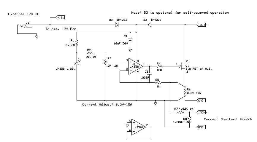
The 1.25V reference diode, 15K resistor, and 10K pot develop a
stable 0 to 0.5V. The single-supply op-amp and FET apply the voltage
to the 0.05 ohm resistor. 0.5V across 0.05 ohms is 10A maximum. You
can parallel multiple larger resistor values if you have trouble
finding a 0.05 ohm 10W resistor. To build a 5A load, use a 0.1 ohm,
5W resistor instead. The only trick in building this is to wire the
high current path with heavy gauge (16GA or more) wire and treat the
0.05 ohm resistor as a 4-wire device: heavy traces for the high
current path, lighter wires soldered to the leads near the body for
the voltage measure path. Here is the ExpressPCB
schematic. and the .PDF. version.
For extra credit, use the unused op-amp and a thermistor to detect
when the heat sink gets hot and turn the fan on. The circuit as
shown shouldn't be used at more than 18V or so since the full supply
can be applied to the FET gate, These are usually rated for 20V max.
By removing D3 and always using the external 12V supply, this
limitation is removed and the voltage can go up to anything the FET
can handle. Watch out for maximum power of the FET though. And
remember to de-rate the FET power at high temperatures.
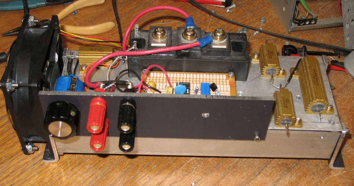
The top binding posts are for the load and the bottom ones for a
current monitor via a DMM. The 3 resistors on the right are just
spares. Note the big black IGBT in the background, this is in place
of the FET in the schematic, but a couple of high power TO-220 or
larger N-FETs in parallel will do fine. The big aluminum block is a
surplus heat sink with its fins facing down. The brackets on the end
keep it somewhat thermally isolated from the bench. With the fan, I
have run this beast at 24V and 10A: 240W for short periods of time.
A real lab supply design
A real lab supply can output a precision voltage or current down to
0V and 0A. It has an accurate meter and nice front panel controls.
This is more than a mere uA723 can provide. I had the brainstorm to
replace the '723 with a small board of precision electronics. I
unsoldered the '723 on this supply, and replaced it with a socket.
Then the functions of the '723 were replaced with a radio-shack
proto board via a 14 pin ribbon cable. Here is the board cabled to
an old Power-One supply. Some minor components changes on the supply
are needed to make this work on any supply. The divider resistors on
the supply need to be scaled or adjusted (or bypassed) to provide
+5V full scale. The foldback current sense circuit needs to be
bypassed. Just remove all the resistors so that pins 2 and 3 of the
'723 connect directly to the current sense resistor.
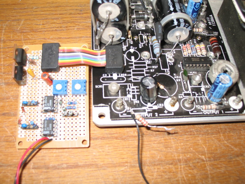
This supply was originally designed to provide +5V at 3A and +30V
unregulated at 2.5A I bought it expressly to build a lab supply out
of it someday. On the +5V side (Output 1) I removed the overvoltage
SCR and added one resistor to allow the output voltage to go down to
+3V. More and more of my projects run off +3.3V.
Output 2 contained the transformer winding, rectifier diodes and
filter caps only. It used a wire to bypass all the regulator
circuitry and connect the + unregulated supply directly to the
output. Note that all the regulation components are missing. I
removed the wire, added a .25 ohm shunt resistor, bypassed the
trimpot, and added a TO-3 NPN transistor. I also added a 100uF 50V
output capacitor. The remaining circuitry is on the perf board and
is shown on this .PDF schematic. This
is the first prototype of this circuit. It works as follows:
There are two control loops, one for voltage and one for current.
Each control loop uses a measurement circuit, and an integrator. A
power stage drives the output. Diodes are used to select either the
voltage or the current integrator to control the output, depending
which is in range. Either integrator can pull the output low if the
output tries to go above its limit. The current sense consists of a
differential x10 amplifier to bring the 0.5V signal across the
current sense resistor to +5V full scale. Its common mode rejection
needs to be very good, like 80dB in order accurately measure the
small voltage across the shunt while the output voltage varies from
0 to full scale. To measure CMRR, unload the power supply (0
current) and see what the meter reads. Then vary the power supply
voltage and see how it changes. The ratio of voltage change to meter
change is CMRR. To build it with readily available parts requires
that the ratio of its 2 pairs of 10K / 100K resistors be matched
precisely, better than 0.1%. You can do this with a 4 1/2 digit DMM
which will resolve the resistors to one part in 10,000. Or wire up a
whetstone bridge driven from a 10-12V power supply, and use your 3
1/2 digit DMM on the mV range for the null measurement.
You also need the op-amp to have good CMRR and be able to handle the
full unregulated voltage. (See the LT1013 below.)
The voltage sense circuit consists of a simple voltage divider. A
goal of both these circuits is to scale both signals to 0 to 5V (or
whatever reference voltage) full scale. That way they can be
measured precisely with a simple ground-referenced DMM or A/D. That
way the current and voltage adjust pots also operate off the same
reference voltage.
It did work OK, but it had a few problems. The current sense
amplifier output cannot go all the way to 0, and neither could the
supply output. This is due to the LM358 inability to pull its output
to ground. Also to switch from voltage to current control and back,
the integrator outputs need to slew the full power supply voltage of
about +40V in order to take control. This takes time and in response
to a large current change, the output will droop or rise (kick)
while this is happening. Also LM358As used are only rated for +32V
operation and I was using them at +40V. So they are probably not
long for this world.So I changed the op-amps to LT1013s which can
handle 44V. The ability to go to 0V is pretty important. since when
you short the output with a current meter to set the current, the
loop must regulate with 0 output volts. So I added 2 series diodes
between the regulator and the TO-220 driver transistor. This did the
trick. On this early proto I was wiling to live with the current
measure not going all the way to 0. A 1K resistor from the current
amp to GND would help a bit here. But at full current (5 V out) the
op-amp would dissipate 5mA X 40V = 200mW and get hot. Not terrible,
but not ideal.
One fix for the 0 voltage and current problems is to build a low
current negative (-5V) supply for the op-amps. Another is to bias
the current measurement opamp so 0 current is actually +0.5V or so,
but this complicates the A/D or DPM design. The integrators and
voltage amp can be operated from a lower supply voltage, like +12V
to reduce their slew times. Then this lower voltage can be amplified
up to the required output voltage by an additional amplifier. But
the current sense amp and the output amp cannot operate from lower
voltages. Fortunately there is a nice part, the LT1013, a reasonably
priced, precision, dual, single supply opamp that can handle up to
44V. Also I want an LED to tell me when the supply is in current
limit mode. The difference between the voltage at the output of the
integrators tells this and a comparator will do the job.
I don't mind hand-wiring a simple first proto to prove out a
concept, but when it gets complicated with support circuitry, or I
need to build more, not so much. So my plan is to build an
ExpressPCB to do this. The first version will prove out all the
analog stuff and will probably use an LCD DPM to do the monitoring.
Here are the original schematic, PDF Schematic and PCB artwork so far. I added a +12V
and -5V supply, limited the range of the integrator opamps to +12V,
changed the op-amps that run off -5 and +35 to LT1013s which can
handle up to 44V. The design supports either a single DPM with a
switch to allow it to read either Volts or Amps, or 2 DPMs, one each
for current and voltage. It supports an LED to show when it is in
current limit mode. The layout uses just 1/2 of an ExpressPCB. The
right half can be a copy of the design (if you need 6 boards) or can
be anything else you can fit in the area. ExpressPCB only allows 350
holes on a mini-board, and this design is right up to that limit. If
you add anything you may have too remove something also.
For the +12V regulator, I used a LM317 adjustable regulator. These
can handle the higher input voltage. The LT1013 with a -5V supply is
specified for 44 - 5 = +39V. This is fine for a +15V supply but a
+24V supply will sometimes have its raw DC as high as +40V. Then
with a line surge, bad things could happen. A 5V zener in series
between the V+ and the op-amp supply would do the trick.
There is an effect called "integrator wind-up" where a control loop
takes extra time to respond to a change because the integrator has
gone off scale in one direction and then needs to integrate all the
way in the other direction in order to regain control. With a power
supply like this, let's say a load is applied that causes the
current limit to take control. When in current limit, the voltage
integrator goes to its + full scale. Then if the load is suddenly
removed, the current integrator will integrates up until the voltage
integrator comes back down to take control. This takes time and
causes a jump or overshoot in the output voltage. There are many
strategies for eliminating integrator windup. One is to simply
reduce the output voltage range of the integrators. The integrators
need not rise above the maximum control setpoint of the supply. The
integrators are powered by the +12V supply. It may be desirable to
reduce this voltage in order to reduce wind-up. So having an
adjustable regulator here might be a good thing.
When multiple output transistors / shunt resistors are used, one
could simply sense current from one shunt and multiply it times the
number of shunts. But this approach won't be very accurate. How to
measure the current from several shunt resistors and sum them up
while still maintaining the resistor matching required for high
CMRR? I didn't want to build multiple high CMRR amps so I came up
with a simple resistor network to manage this. The magic value is
500 ohms. By adding a 500 ohm resistor to each 10K, the CMRR is
still well balanced. To sum 2 shunt resistors, replace the + side
500 ohm resistor with two 1Ks, one for each resistor. For 3 shunts,
use 3 x 1500 ohms. for 4, use 4 x 2.00K. All these resistors in
parallel equal 500 ohms. All these are available in 1% except for
the 500 ohms. But 499 ohms is close enough. Even better, these
multiple resistors can each be sky-wired directly to the shunt
resistors and only their common terminal needs to be returned to the
10K of the current measure amp.
When you are done building this dandy controller, it may be apparent
to you that the power-one supply is not all that necessary. All
we're really using of it is the transformer, rectifier, TO-3,
heat-sink (case) and filter cap. These parts can be bought or
scrounged separately, mounted to sheet metal pretty easily and the
Power-one board can be pretty much eliminated. Advantages of this
approach? Since you need to derate the Power-one current spec by
about 2/3 to 1/2 when building a lab supply, the transformer, diodes
and cap are over-designed, meaning overly large. The transistor is
OK, but the heat sinking of the power-one case will be too light.
Adding a real finned heat sink and mounting it on the rear of your
package will be a big improvement.
Power Supply Dynamics
The dynamic or transient response of a power supply is design
dependent. Raw Power-one supplies are pretty simple. Their frequency
response is primarily dictated by the output filter capacitor plus
the uA723 compensation capacitor. Complicated a bit by the fact that
the output transistor can charge the output but not easily discharge
it. The supply is designed to provide a steady DC controlled by a
trimpot, so as long as the output tracks the trimpot during
adjustment, all is good. A lab supply has a much wider range of
adjustment. And a programmable lab supply can jump from one voltage
setting to another pretty quickly.
Another aspect of transient behavior is the response of the current
limit circuit. On a power-one, the speed of the output to drop
during current limit and to recover after isn't real important.
However you don't want the output voltage to overshoot much when the
output current is removed. With a lab supply intended to operate
regularly in both constant current and constant voltage modes, the
circuit should be able to switch modes cleanly. The circuit that
does this is sometimes called a 'crossover' since it automatically
switches from constant current to constant voltage. One simple way
to build this is with two integrators, one for voltage and one for
current control. Then the output of each integrator is simply analog
'or-ed' with two common-anode diodes and a pull-up resistor. The
lowest integrator voltage limits the output voltage. If the voltage
output is higher than the voltage setting, then the voltage
integrator slews down to reduce the output. Same with the current
integrator. Lowest integrator wins.
This works well except for one important case: When the unit is in
current limit mode, the voltage integrator goes to it's maximum
value, set by the integrator's supply voltage or by some limiter
circuit if present. Then if the current load is quickly removed, the
current integrator slews up to increase the output voltage. But the
voltage integrator can't begin slewing downward until the output is
above the setpoints. The net result is that it takes time for the
voltage integrator to respond and the output overshoots it's
setpoint. The 2-integrator circuit I built causes about a 1V
overshoot. This extra 1V can damage sensitive circuits. Not good.
The resistors in series with the integrator caps help. They add a
"P" or proportional term to the loop so an instantaneous change in
an output ( I or V) causes a quicker response of the integrator
output. A "D" or derivative term can also help here. But it cannot
be corrected for all cases.
A more elegant solution is to use a single integrator with a
'crossover at it's input. The charge on the single integrator
controls the output. The single integrator either integrates voltage
error or the current error with some simple decision logic. The
voltage error normally controls the integrator. But if the current
output is above the current setpoint, the current error controls it.
This can be done pretty simply with a 'precision diode' or absolute
value circuit.
Packaging a lab supply
Packaging homebrew projects is always a challenge. You want them to
look decent but don't want to put infinite work into the case.
Trying to jam your latest creation into an off-the-shelf box can be
frustrating. One part won't quite fit so you need to go to the next
bigger size box which now is mostly filled with air. The box looks,
well, off-the-shelf. For lab projects or prototypes, any old box or
even no box can be used. In the early days I built boxes from wood
and sheet metal. Plywood for a quick-and-dirty, oak and plexiglas
for something that lives in the house, and teak for the boat. But
unfortunately, the seventies are over. One advantage of wood, is
that it can be machined with a table saw or router, it can be
screwed into. It can be painted or varnished. Lately I've been
looking at "King Starboard" and other plastics. Starboard is being
widely accepted as an alternative to wood on boats since it can be
machined like wood and never needs refinishing. It's available in
marine stores in mostly white, and on-line in black, gray, white and
off-whites. Plexiglas (lexan is good for machining, acrylic is too
brittle) is also available in clear and other colors. Contact your
local plastics dealer or buy scraps on Ebay.
My box concept: 2 vertical sides of 3/8" or 1/2" plastic, machined
with slots for the top and bottom, and and threaded for screws for
the front and rear. The other panels are 1/16" or so sheet aluminum
either painted or left natural. The front can be 0.060, 0.090 or
1/8" aluminum to give a sense of strength. 1/8" aluminum rack
panels are one way to go. These can be obtained in a nice brushed
aluminum finish for a price. Heights are standard 1U/2U/3U ...
sizes. The front of this design overlaps the sides, top, and bottom
to hide the plastic from the front. I'd round those sharp corners.
Use contrasting black socket head (allen) screws and it will look
pretty decent. Here's a .pdf
drawing of what I have in mind. Visio is great for seeing if
things will fit. Measure the components of your project, draw them
as simple shapes, then arrange them to fit the enclosure, or change
the enclosure size to fit the objects. You can do a nice 2D
dimensioned drawing with Visio.
The real deal
Here is the final HC15-3 power supply. This one is designed to
output up to +18V at 2A.
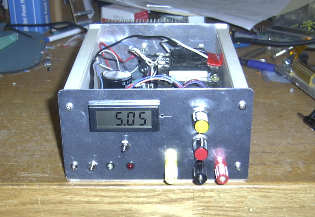
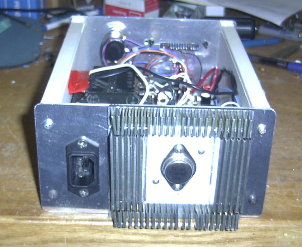
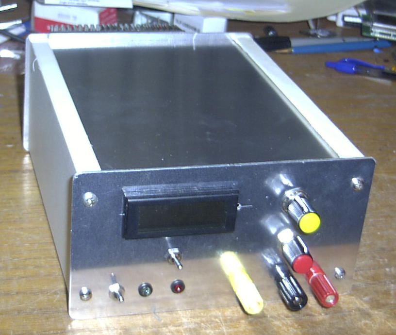
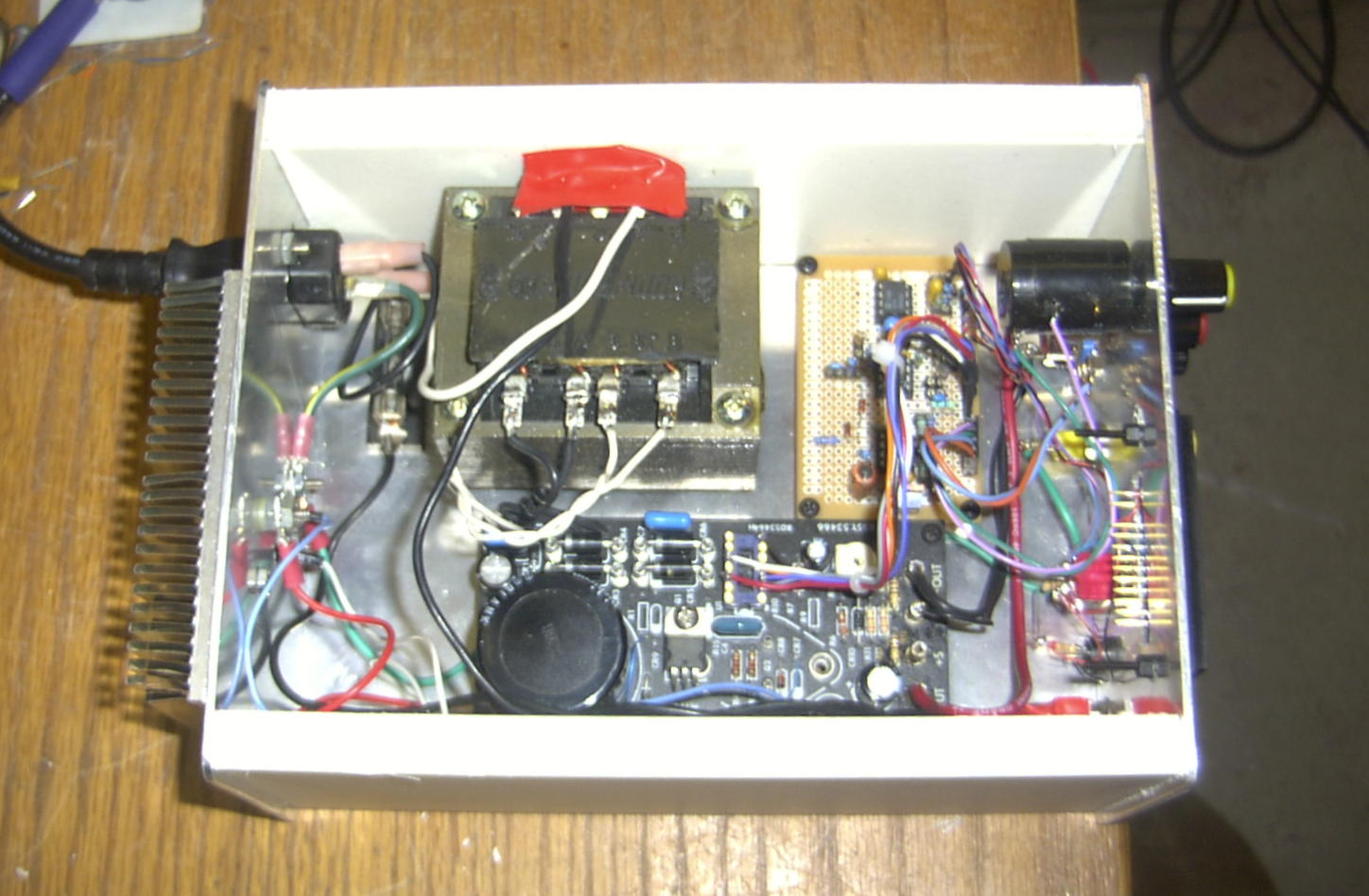
For the low voltage HC15, I was able to build a nice simple 4 op-amp
circuit. Two 8 pin DIP op-amps, a +5V regulator, and a -5V converter
fit nicely on a small RS breadboard. The design does 0.0 to 18V at
up to 2A. The transformer and board came directly from the HC15-3.
The DPM is a Modutec 0-2V model.
The Mods to the HC15-3 board are as follows:
Remove the uA723 regulator and replace it with a nice
machined-contact IC socket.
Bypass the boost power supply. This requires removing R1 (220 ohms)
and adding a wire to connect V+ to VC.
The clever current limit was bypassed: remove the current limit pot
R5 and CR7, then wire U1 pin2 to the + side of the current limit
resistor R2.
The voltage divider was bypassed: remove R9 and R10 and adjust R8
for it's minimum value.
Remove the output transitor Q2, bolt it to the heat sink (with
proper insulating washers) and run wires from the board E-B-C
connections to the transistor on the heat sink.
Check your wiring. Make sure:
The power board + Sense pin is
connected to the uA723 pin 4
Pin 3 is connected to Vout+
Pin 2 is connected to the + (input) side of R2
Without the uA723 installed, power it up and check that V+ and VC
are both about +23V
After turning off the AC power, you'll need to discharge the cap
with a 10 to 220 ohm resistor from V+ to VS- (GND) to safely
proceed.
Instead of a crimp-style DIP cable, this time I built a my own cable
from a 14 pin DIP header and six #24 wires. All you need is V+ (12),
IN- (4),V- (7), ILIM+ (2), ILIM- (3) and OUT(10). When soldering to
a DIP header, put it in a socket to prevent the heat from melting
the body.
The DPM is a 1.999V range unit with a +5V power supply. A voltage
divider measures the V out and divides by 10.0. I use the gain
adjustment on the DPM to calibrate the voltage meter range. Make the
supply DPM agree with an external DMM. Then to calibrate current,
short the output through a DMM set to 2A or 10A. Set the current
limit pot to about 1.5A, and adjust R20 till the DMM and the DPM
agree I used a fixed value for R20 but a 5K trimpot would be better.
The voltage adjust is a nice 100K 10-turn pot. The current pot is 1
turn only. I was too cheap to use another $10 10-turn pot. The heat
sink is surplus, intended for a big Apex power amplifier module and
re-drilled for a TO-3. The sheet metal was scraps, and the sides are
1/2" King Starboard in a beige color.
Here's the schematic in .PDF and
in Express. It's a simple 2
integrator design that uses a -2.5V reference voltage. The adjust
pots balance against fixed resistors that control the full scale
voltage (R14) and current (R18) values. The integrators use GND as
their + input, and output up to +3.3V. The gating diodes add +.7V to
make +4V maximum. This is multiplied by the 5X amplifier to make
+20V max. The output stage needs 2 Vbe drops (1.4V) + .25V for the
shunt or about 1.7V. So the max output is about 20 - 1.7V, just over
the required 18V. In reality the LM358 integrators will output a bit
more voltage since their output is being pulled high by the diode
and 10K pull-up.
The Current limit LED works reasonably well tied to the Voltage
integrator and +5V. In current limit mode, the voltage integrator
loses control and goes low. The light is a bit dim when the voltage
out is above about +15V, but otherwise works fine.
Since the max V is only +18V and the max I is 2A, the DPM design is
simple. The ranges can be 19.99V and 1.999A. it means you can't read
over 1.999A though, the meter goes into over-range. But 1.999 is
close enough to 2.000.
03/08 Update: VI Design / Battery tester
The power supply was so successful I decided to go to the next
level: a computer controlled voltage / current source and sink. This
is sometimes called a VI. It can sink or source current, be
adjusted, turned on and off so it can charge or discharge (test) any
battery. I worked at an ATE company, Teradyne and we built very
high quality VIs for semiconductor testing. A proper VI used in ATE
probably has many decades of current ranging from micro Amps to Amps
and and is a very precise instrument. They are generally
'four-quadrant' devices that can sink or source current at + or -
voltages. This one is 2 quadrant, no negative voltages. And it has
just one current and one voltage range.
A simple LabView program controls it. No Power-One components this
time. 0 to 20V, +3A source or -5A sink. The control loop is similar
to the one on the PowerOne hack, but uses an additional integrator
to control the sink current. I use a small National Instruments USB
data acquisition (DAQ) unit to control and measure it. The DAQ has 2
0-5V DACs and 14 bit ADCs. Mine is the 14 bit USB6009 (but the 12
bit USB6008 ($149) will also work fine. The output stage uses two
big TO3 transistors on a heat sink. One NPN to source current and
one PNP to sink it. Here's the schematic in ExpressPCB format. and in PDF
If the DAQ had three D/As I would use the third to independently
control sink (negative) current, but with just two, one DAC is used
to control both source and sink at +/- the same setting. So far it
hasn't been much of a limitation. The first DAC controls voltage.
One limitation of this system is that this DAQ (like most low-cost
USB DAQs) is grounded to the PC, so the load must essentially be
floating. Not a problem with a battery, but as a power supply or
load, the grounding can cause errors if there are other paths to
ground. Dave's first rule of analog problems: "It's always the
ground."
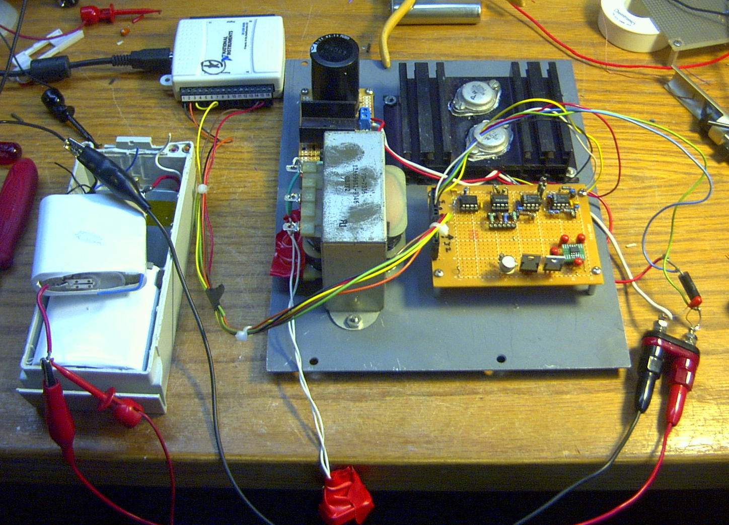
The control circuitry is built on a large RadioShack board. Behind
the transformer is another small RadioShack board with the rectifier
diode and filter cap. The output connectors and the shunt resistor
are on the right. The NI USB DAQ is on the upper left. The big white
thing on the left is a lithium battery being tested. The white
twisted wires on the bottom is the not-so-safe AC input. It is fused
and insulated however. The transformer is about 30VAC, 3A. the final
unit will have the AC in and a cooling fan on the rear, hopefully a
DMM or two on the front, and the ability to operate it stand-alone
(via knobs) or remotely via the LabView DAQ.
The DAQ is about 0.5% accurate and I wanted better, so I calibrated
it. Unfortunately NI doesn't support any type of calibration for
these cheapie DAQs, so I was on my own. I measured zero and full
scale voltage on the ADCs and DACs and calculated the appropriate
corrections. Works great and gives be about +/- 0.1% voltage
accuracy. But every channel and voltage range needs calibration, and
when you change DAQs, the numbers all need to change. I only use one
voltage range and 2 inputs so the task wasn't bad.
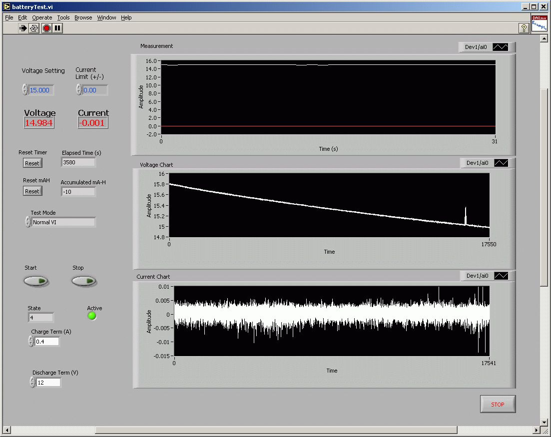
Here is a screen shot of the LabView application running. It can
operate as a normal VI, or can charge or discharge a battery,
terminating on a specified condition. The top plot is the
instantaneous voltage and current. The bottom plots are voltage and
current long-term trends. There are two reset buttons to reset
either the time or the accumulated charge. This indicator reads +
when the VI is sourcing current and - when it drains current. Here
is the LabView code.
For charge termination control, many batteries want to be charged at
a constant current until a voltage limit is reached, then monitor
the current until it drops to a certain value. This works well for
Lithiums, lead acid, and ni-cads. Be careful not to exceed the
current and voltage limits on batteries or they will be damaged or
explode. A proper high current charger or tester would also monitor
temperature and time and terminate if either of these exceeded
limits. Exercises left to the student.
For discharge testing, the VI is set to apply a constant current
load and the LabView program monitors the voltage. LabView
terminates when the voltage drops below a threshold so as not to
damage the battery. LabView also accumulates the current every
second to arrive at the battery capacity. I accumulate mA-Seconds
and scale it to display mA-Hours.
Lithiums are the pickiest of all. Charge voltage is generally 4.20V
per cell, not 4.25. Over charge and they die. Discharge below 3V and
they die. Too much charge current and they die. Look a them
cross-eyed and they die. Don't balance the voltages properly and
they die. Or worse, explode.
I have taken apart many old laptop batteries to scavenge their 16450
cells. With careful disassembly and very careful unsoldering, it can
be done. The key word is "old". New ones are too valuable to take
apart, and old ones lose so much of their capacity that they are not
useful. So this has been an un-fruitful endeavor. Finally I found
some nice surplus oblong-shaped lithium cells from Saft, about the
size of three 16450s. They test at about 5000mAH and are currently
powering my bike light. .
12/09 Update: Boat Anchor or Audio Amplifier?
I just obtained a Power-One F-24-12-A. This giant, full rack
width supply is 24V at 12A or 28V at 10A. It has nine TO3
devices and 4 heat sinks to dissipate / waste all the power it
needs. It also specifies a 50CFM fan to fulfill its destiny as a
space heater. I makes little sense to use a 300W linear supply when
a switcher would be 1/10 the volume and 85% efficient vs. maybe 60%
efficient. But free was free. The last time I looked there
were a handful of these beasts on Ebay for ~$50.
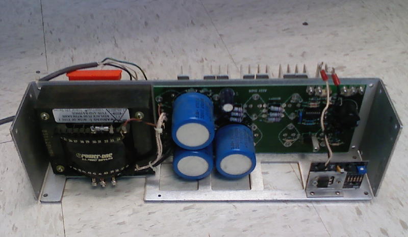 It would make a pretty poor lab supply. A proper lab
supply of more than 100W uses some kind of pre-regulator to reduce
the voltage drop and power dissipation in the pass element. Many
such as the original HP supplies used SCR stages to pre-regulate and
as such are very efficient as well as clean. I love my HP
6286A. 20V at 10A and it is barely warm when outputting high
currents at low voltages.
My thinking is to use just the unregulated section of the F-24-12-A
to power an audio amp. It would have to be rewired for +/-
operation. Since the unregulated section was about 30-35V, a decent
voltage for an audio amp, this could work. But alas, the transformer
is not center tapped. It is tapped, but only to supply either 24V or
28V raw. A jumper on the board is used to select the tap. So it
cannot output full wave DC to both a + and - supply. Too bad. And
the filter caps are three at 13,000 uF 50V. They would be fine for
an audio amp, but three? You need either 2 or 4. And the diodes are
TO3; first time I have ever seen diodes in a TO3 case. To build the
diode bridge, there are two different TO3 diode part numbers, one
common anode and one common cathode.
A toroidal transformer is best for an audio amp. Toroids throw off
lower magnetic fields which can induce hum in low level audio
stages. But this freebie is staring at me, daring me to give it new
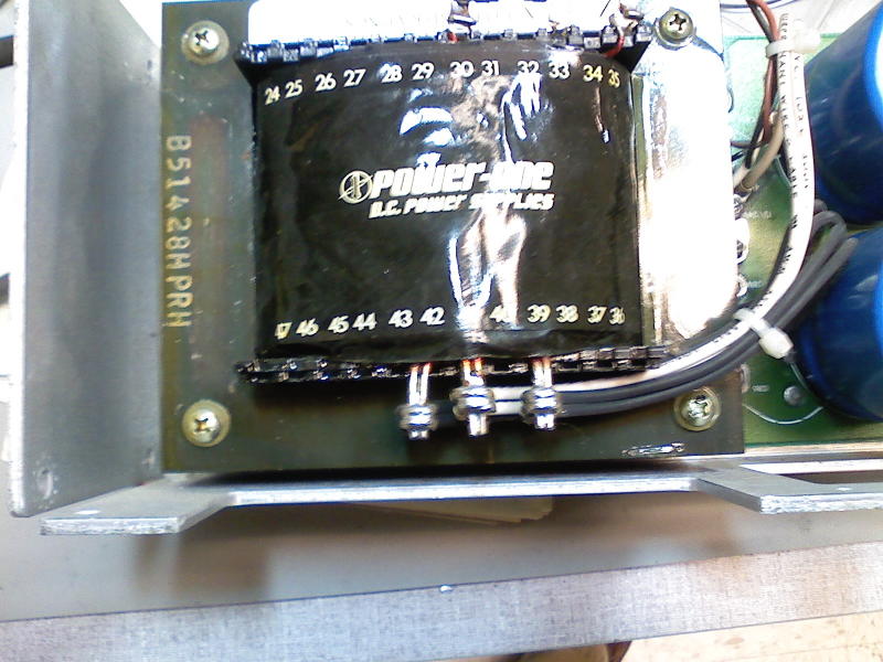
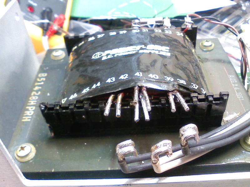
life. I wonder if this transformer's windings are bifilar, two
windings in parallel and can be somehow separated? Sure enough, they
are bifilar and the windings can be easily separated. Check it out.
Use solder wick to get every speck of solder off the leads. Then use
small pieces of heat shrink pushed under the transformer insulation
to prevent shorts.


There are two 28VAC windings in parallel, in series with two
3VAC windings in parallel. The 3V is added to the 28V to provide
extra volts for the 28VDC option. This means that the transformer
can provide either 28VAC, 31VAC, or if you wire the 3V in series
with the 28V, but with reversed polarity, 28-3 = 25VAC. And
there are two of each of these that can be rewired in series for a
center tapped configuration. Cool! The AC options are 25, 28 0r 31V
(50, 56, 61 VCT). DC is 1.414 * the AC, minus about 1V for the
diode. The loaded supply is about 3 volts less. I measured this with
a 3A DC load. Then you lose about 4V in the filter caps due to
ripple and the output transistors of a typical amp design , the
power into an 8 ohm speaker is about (((VDC - 4) / 1.414 )^2) / 8.
This .pdf schematic shows the
final design with the transformer connection options. Here is the ExpressPCB .SCH File.
VAC
|
Wiring
|
VDC
No Load
(1.4* VAC) - 1
|
VDC w/ Load
|
Power estimate into 8 ohms
(((VDC - 4) / 1.414) ^2 ) / 8
|
25VAC: 50VCT
|
28V - 3V
|
+/- 33 |
+/- 30
|
40W
|
28VAC: 56VCT
|
28V, no 3V
|
+/- 37
|
+/- 34
|
53W
|
31VAC: 62VCT
|
28V + 3V |
+/- 41
|
+/- 37
|
64W
|
The windings are good for about 350W, so a guess at the total audio
output is about 250W. I have wanted to build a multi channel amp
based on the National LM3886 for years. The LM3886 is a decent 50W
part, so I'll probably go with the middle voltage option. I'll saw
the PC board and the bracket just to the right of the 2 caps. That
will give me a transformer, the diodes and two caps, just the raw DC
supplies, and will remove all the regulator stuff. The board
is mounted to the chassis via the TO3 hardware, so leave the diodes
and maybe the next row of TO3s just for mounting.
The unit came apart fairly easily. The 4 heat sinks and 7 of the 9
TO3s just unscrewed. The 3 big caps just unscrewed with an allen
wrench. The two TO3 diodes were a challenge to unsolder, They
have big leads and the board holes are a tight fit. After sucking
away most of the solder on top, I had to pry the part off one lead
at a time. Two big soldering irons, one on each lead would have
helped.
I used a Sharpie to mark where the copper cuts and jumps need to go.
The heavy copper layer was too thick to easily cut with an Xacto so
I used a utility knife to make 2 cuts and then peeled off the copper
strip between the slices. For wire I used #16.
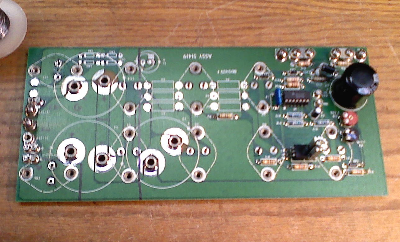
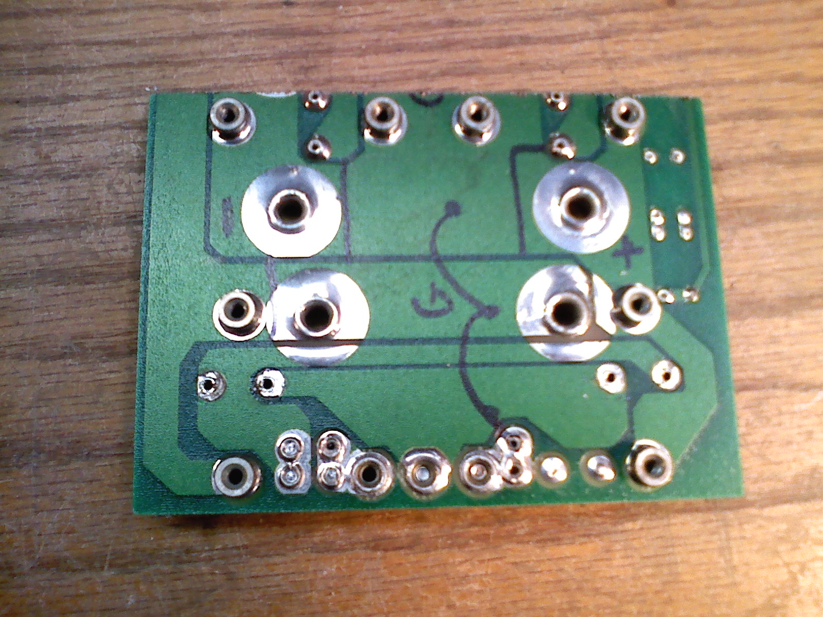
Here is the board prior to being cut in two.

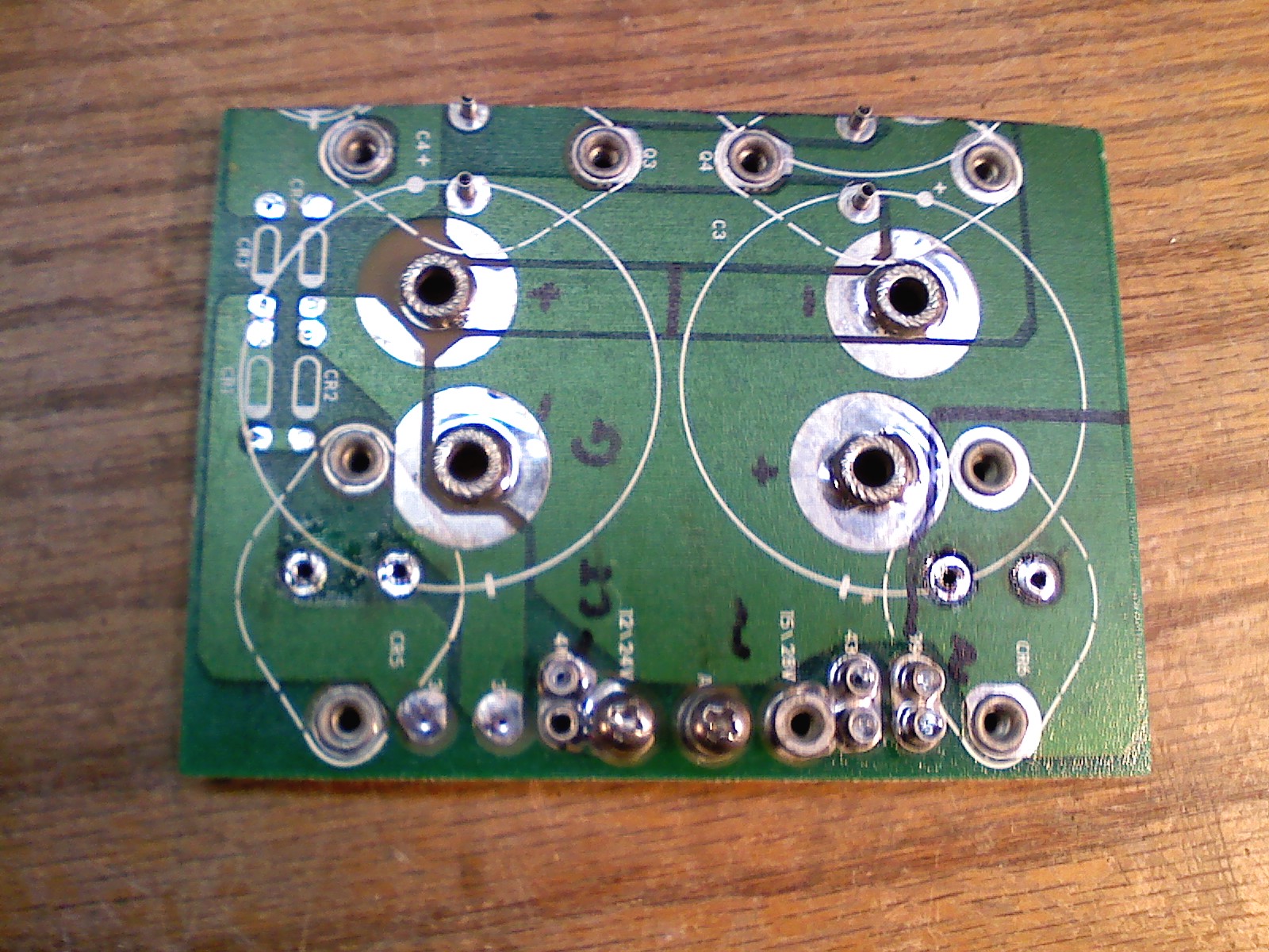
And after, showing the board top and bottom. After cutting the
traces and adding the wires, make sure to continuity check every
connection.


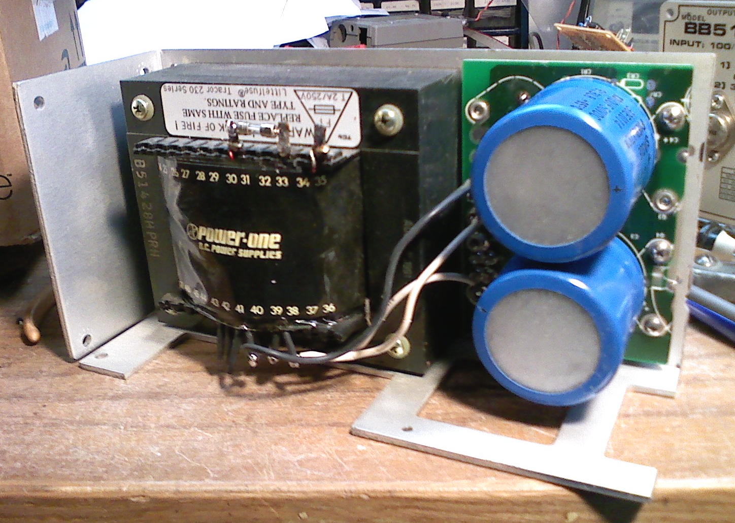
Here is the unit all built up. I kept the screws of the right-most
TO3 transistors to use as convenient mounting screws (1) and output
terminals (3). You can determine if the output is to be grounded or
not at the chassis. Use an insulating shoulder washer for the ground
screw to keep is isolated. Remove the insulation to ground it.
Typically in an audio amp up want to ground the power supply at the
amplifier, not the power supply. This requires using the original
TO3 insulators under these terminals.
Mark the TO3 diodes to maks sure you get the right one back in the
right place. You can use a DMM on diode range to identify their
polarity. And DO NOT FORGET
to install C3 backwards from the marking on the PCB: + side goes to GND. I should
have crossed out the original "+" on the board.
With no 3V windings connected, the AC voltage is 28VAC. Output
voltage is +/- 37V, no load, and +/- 34V with a 3A DC load. Ripple
is about 1.5Vp-p at 3A. It's all ready to power a nice audio amp.
For the chassis, after removing the heat sinks, board and
transformer, I marked it and cut it with a band saw. A jig saw or a
hack saw plus patience would also do it. The heat sinks are mounted
to pressed-in studs which remove with a light hammer blow. With the
lighter load of an audio amp, the diodes should generate little heat
and so no heat sink is required. The chassis alone is a fine heat
sink. You could also remove the left end plate since it is unlikely
to be used for mounting, and it provides no added strength. You
could also kill the chassis bracket completely and just mount the
board and transformer to your chassis. You'd need heavy spacers and
longer screws for the transformer. You'd need to replicate the
mounting holes, but the original chassis could be used as a fine
template.
The three unused terminals on top of the transformer are for the
original boost supply. This 8.5VAC winding could be used to power
some additional logic or analog circuits. I removed the diodes and
the cap that they were connected to.

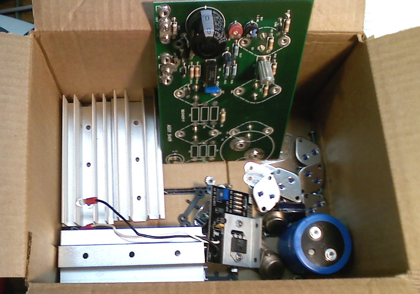
Here are the leftover parts, not including the other half of the
cut-off chassis. The chassis, transistors, big cap, and remaining
1/2 board could still be built up as a lab supply, but would need a
transformer and diodes. By the way, the 6 removed T03 series pass
transistors are 2N3773s, 140V NPNs. 4 of them would make an
nice audio amp quasi-complementary output stage. The .22 ohm ballast
resistors and heat sink hardware can also be used.

Back to Dave's Home Page
This page was last updated 7/24/10


 It would make a pretty poor lab supply. A proper lab
supply of more than 100W uses some kind of pre-regulator to reduce
the voltage drop and power dissipation in the pass element. Many
such as the original HP supplies used SCR stages to pre-regulate and
as such are very efficient as well as clean. I love my HP
6286A. 20V at 10A and it is barely warm when outputting high
currents at low voltages.